 | –≠–ª–µ–∫—Ç—Ä–æ–Ω–Ω—ã–π –∫–æ–º–ø–æ–Ω–µ–Ω—Ç: NE5539N | –°–∫–∞—á–∞—Ç—å:  PDF PDF  ZIP ZIP |
Philips Semiconductors RF Communications Products
Product specification
NE/SE5539
High frequency operational amplifier
229
April 15, 1992
853-0814 06456
DESCRIPTION
The NE/SE5539 is a very wide bandwidth, high slew rate, monolithic
operational amplifier for use in video amplifiers, RF amplifiers, and
extremely high slew rate amplifiers.
Emitter-follower inputs provide a true differential input impedance
device. Proper external compensation will allow design operation
over a wide range of closed-loop gains, both inverting and
non-inverting, to meet specific design requirements.
FEATURES
∑
Bandwidth
≠ Unity gain - 350MHz
≠ Full power - 48MHz
≠ GBW - 1.2GHz at 17dB
∑
Slew rate: 600/V
µ
s
∑
A
VOL
: 52dB typical
∑
Low noise - 4nV
Hz typical
∑
MIL-STD processing available
APPLICATIONS
∑
High speed datacom
∑
Video monitors & TV
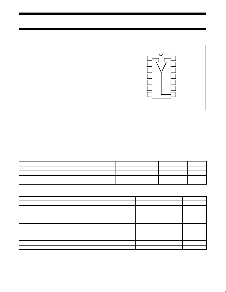
PIN CONFIGURATION
+ INPUT
NC
-VSUPPLY
- INPUT
NC
NC
NC
VOSADJ
/
AV ADJ
GROUND
+V
NC
OUTPUT
D, F, N Packages
NC
1
2
3
4
5
6
7
14
13
12
11
10
9
8
Top View
FREQUENCY
COMPENS.
+
≠
∑
Satellite communications
∑
Image processing
∑
RF instrumentation & oscillators
∑
Magnetic storage
∑
Military communications
ORDERING INFORMATION
DESCRIPTION
TEMPERATURE RANGE
ORDER CODE
DWG #
14-Pin Plastic Dual In-Line Package (DIP)
0 to +70
∞
C
NE5539N
0405B
14-Pin Plastic Small Outline (SO) package
0 to +70
∞
C
NE5539D
0175D
14-Pin Ceramic Dual In-Line Package
0 to +70
∞
C
NE5539F
0581B
14-Pin Ceramic Dual In-Line Package
-55 to +125
∞
C
SE5539F
0581B
ABSOLUTE MAXIMUM RATINGS
1
SYMBOL
PARAMETER
RATING
UNITS
V
CC
Supply voltage
±
12
V
P
DMAX
Maximum power dissipation,
T
A
= 25
∞
C (still-air)
2
F package
N package
D package
1.17
1.45
0.99
W
W
W
T
A
Operating temperature range
NE
SE
0 to 70
-55 to +125
∞
C
∞
C
T
STG
Storage temperature range
-65 to +150
∞
C
T
J
Max junction temperature
150
∞
C
T
SOLD
Lead soldering temperature (10sec max)
+300
∞
C
NOTES:
1. Differential input voltage should not exceed 0.25V to prevent excesive input bias current and common-mode voltage 2.5V. These voltage
limits may be exceeded if current is limited to less than 10mA.
2. Derate above 25
∞
C, at the following rates:
F package at 9.3mW/
∞
C
N package at 11.6mW/
∞
C
D package at 7.9mW/
∞
C

Philips Semiconductors RF Communications Products
Product specification
NE/SE5539
High frequency operational amplifier
April 15, 1992
230
EQUIVALENT CIRCUIT
(≠) 14
INVERTING INPUT
(+) 1
NON≠INVERTING
INPUT
5
(3) ≠VCC
(7) GRD
(8) OUTPUT
(10) +VCC
(12) FREQUENCY COMP.
2.2k
R18
R19
R3
R5
R2
R6
R8
Q1
Q2
Q4
Q3
Q6
Q5
Q7
Q8
R20
R1
R4
R21
R9
R10
R7
R17
R16
Q9
Q10
R13
R11
R12
R14
R15
Q11
DC ELECTRICAL CHARACTERISTICS
V
CC
=
±
8V, T
A
= 25
∞
C; unless otherwise specified.
SYMBOL
PARAMETER
TEST CONDITIONS
SE5539
NE5539
UNITS
SYMBOL
PARAMETER
TEST CONDITIONS
MIN
TYP
MAX
MIN
TYP
MAX
UNITS
V
OS
Input offset voltage
V
O
= 0V, R
S
= 100
Over temp
2
5
mV
V
OS
Input offset voltage
V
O
= 0V, R
S
= 100
T
A
= 25
∞
C
2
3
2.5
5
mV
V
OS
/
T
5
5
µ
V/
∞
C
I
OS
Input offset current
Over temp
0.1
3
µ
A
I
OS
Input offset current
T
A
= 25
∞
C
0.1
1
2
µ
A
I
OS
/
T
0.5
0.5
nA/
∞
C
I
B
Input bias current
Over temp
6
25
µ
A
I
B
Input bias current
T
A
= 25
∞
C
5
13
5
20
µ
A
I
B
/
T
10
10
nA/
∞
C
CMRR
Common mode rejection ratio
F = 1kHz, R
S
= 100
, V
CM
±
1.7V
70
80
70
80
dB
CMRR
Common mode rejection ratio
Over temp
70
80
dB
R
IN
Input impedance
100
100
k
R
OUT
Output impedance
10
10

Philips Semiconductors RF Communications Products
Product specification
NE/SE5539
High frequency operational amplifier
April 15, 1992
231
DC ELECTRICAL CHARACTERISTICS (Continued)
V
CC
=
±
8V, T
A
= 25
∞
C; unless otherwise specified.
SYMBOL
PARAMETER
TEST CONDITIONS
SE5539
NE5539
UNITS
SYMBOL
PARAMETER
TEST CONDITIONS
MIN
TYP
MAX
MIN
TYP
MAX
UNITS
V
OUT
Output voltage swing
R
L
= 150
to GND and
470
to -V
CC
+Swing
-Swing
+2.3
-1.7
+2.7
-2.2
V
V
OUT
Output voltage swing
R
L
= 25
to GND
Over temp
+Swing
-Swing
+2.3
-1.5
+3.0
-2.1
V
V
OUT
Output voltage swing
R
L
= 25
to GND
T
A
= 25
∞
C
+Swing
-Swing
+2.5
-2.0
+3.1
-2.7
V
I
CC+
Positive supply current
V
O
= 0, R
1
=
, Over temp
14
18
mA
I
CC+
Positive supply current
V
O
= 0, R
1
=
, T
A
= 25
∞
C
14
17
14
18
mA
I
CC-
Negative supply current
V
O
= 0, R
1
=
, Over temp
11
15
mA
I
CC-
Negative supply current
V
O
= 0, R
1
=
, T
A
= 25
∞
C
11
14
11
15
mA
PSRR
Power supply rejection ratio
V
CC
=
±
1V, Over temp
300
1000
µ
V/V
PSRR
Power supply rejection ratio
V
CC
=
±
1V, T
A
= 25
∞
C
200
1000
µ
V/V
A
VOL
Large signal voltage gain
V
O
= +2.3V, -1.7V, R
L
= 150
to
GND, 470
to -V
CC
47
52
57
dB
A
VOL
Large signal voltage gain
V
O
= +2.3V, -1.7V
Over
temp
dB
A
VOL
Large signal voltage gain
R
L
= 2
to GND
T
A
= 25
∞
C
47
52
57
dB
A
VOL
Large signal voltage gain
V
O
= +2.5V, -2.0V
Over
temp
46
60
dB
A
VOL
Large signal voltage gain
R
L
= 2
to GND
T
A
= 25
∞
C
48
53
58
dB
DC ELECTRICAL CHARACTERISTICS
V
CC
=
±
6V, T
A
= 25
∞
C; unless otherwise specified.
SYMBOL
PARAMETER
TEST CONDITIONS
SE5539
UNITS
SYMBOL
PARAMETER
TEST CONDITIONS
MIN
TYP
MAX
UNITS
V
OS
Input offset voltage
Over temp
2
5
mV
V
OS
Input offset voltage
T
A
= 25
∞
C
2
3
mV
I
OS
Input offset current
Over temp
0.1
3
µ
A
I
OS
Input offset current
T
A
= 25
∞
C
0.1
1
µ
A
I
B
Input bias current
Over temp
5
20
µ
A
I
B
Input bias current
T
A
= 25
∞
C
4
10
µ
A
CMRR
Common-mode rejection ratio
V
CM
=
±
1.3V, R
S
= 100
70
85
dB
I
CC+
Positive supply current
Over temp
11
14
mA
I
CC+
Positive supply current
T
A
= 25
∞
C
11
13
mA
I
CC-
Negative supply current
Over temp
8
11
mA
I
CC-
Negative supply current
T
A
= 25
∞
CmA
8
10
mA
PSRR
Power supply rejection ratio
V
CC
=
±
1V
Over temp
300
1000
µ
V/V
PSRR
Power supply rejection ratio
V
CC
=
±
1V
T
A
= 25
∞
C
µ
V/V
V
OUT
Output voltage swing
Over
+Swing
+1.4
+2.0
V
V
OUT
Output voltage swing
R
L
= 150
to GND
temp
≠Swing
≠1.1
≠1.7
V
V
OUT
Output voltage swing
and 390
to ≠V
CC
T
A
=
+Swing
+1.5
+2.0
V
25
∞
C
≠Swing
≠1.4
≠1.8

Philips Semiconductors RF Communications Products
Product specification
NE/SE5539
High frequency operational amplifier
April 15, 1992
232
AC ELECTRICAL CHARACTERISTICS
V
CC
=
±
8V, R
L
= 150
to GND and 470
to -V
CC
, unless otherwise specified.
SYMBOL
PARAMETER
TEST CONDITIONS
SE5539
NE5539
UNITS
SYMBOL
PARAMETER
TEST CONDITIONS
MIN
TYP
MAX
MIN
TYP
MAX
UNITS
BW
Gain bandwidth product
A
CL
= 7, V
O
= 0.1 V
P-P
1200
1200
MHz
Small signal bandwidth
A
CL
= 2, R
L
= 150
1
110
110
MHz
t
S
Settling time
A
CL
= 2, R
L
= 150
1
15
15
ns
SR
Slew rate
A
CL
= 2, R
L
= 150
1
600
600
V/
µ
s
t
PD
Propagation delay
A
CL
= 2, R
L
= 150
1
7
7
ns
Full power response
A
CL
= 2, R
L
= 150
1
48
48
MHz
Full power response
A
V
= 7, R
L
= 150
1
20
20
MHz
Input noise voltage
R
S
= 50
, 1MHz
4
4
nV/
Hz
Input noise current
1MHz
6
6
pA/
Hz
NOTES:
1. External compensation.
AC ELECTRICAL CHARACTERISTICS
V
CC
=
±
6V, R
L
= 150
to GND and 390
to -V
CC
, unless otherwise specified.
SYMBOL
PARAMETER
TEST CONDITIONS
SE5539
UNITS
SYMBOL
PARAMETER
TEST CONDITIONS
MIN
TYP
MAX
UNITS
BW
Gain bandwidth product
A
CL
= 7
700
MHz
BW
Small signal bandwidth
A
CL
= 2
1
120
MHz
t
S
Settling time
A
CL
= 2
1
23
ns
SR
Slew rate
A
CL
= 2
1
330
V/
µ
s
t
PD
Propagation delay
A
CL
= 2
1
4.5
ns
Full power response
A
CL
= 2
1
20
MHz
NOTES:
1. External compensation.
TYPICAL PERFORMANCE CURVES
NE5539 Open-Loop Phase
NE5539 Open-Loop Gain
0
90
180
270
360
1 MHz
10MHz
100MHz
1GHz
FREQUENCY (Hz)
PHASE (DEG)
60
50
40
30
20
10
0
1 MHz
10MHz
100MHz
1GHz
FREQUENCY (Hz)
GAIN (dB)

Philips Semiconductors RF Communications Products
Product specification
NE/SE5539
High frequency operational amplifier
April 15, 1992
233
TYPICAL PERFORMANCE CURVES
(Continued)
dB BELOW REF
Power Bandwidth (SE)
Power Bandwidth (NE)
SE5539 Open-Loop Gain vs Frequency
Power Bandwidth
SE5539 Open-Loop Phase vs Frequency
Gain Bandwidth Product vs Frequency
5
4
3
2
1
GAIN (--2)
VCC = +8V
RL = 2k
3dB B.W
1 MHz
10MHz
100MHz
300Mhz
p≠p OUTPUT (V)
FREQUENCY (Hz)
3dB B.W.
1 MHz
10MHz
100MHz
300Mhz
FREQUENCY (Hz)
p≠p OUTPUT (V)
4
3
2
1
0
VCC = +6V
RL = 150k
GAIN (--2)
1 MHz
10MHz
100MHz
300Mhz
FREQUENCY (Hz)
VCC = +6V
RL = 126
0
o
50
40
30
20
10
GAIN (dB)
22
20
18
16
14
12
1MHz
10MHz
100MHz
FREQUENCY (Hz)
GAIN (dB)
3dB BANDWIDTH
3dB BANDWIDTH
AV = X7.5
AV = X10
VCC =
±
6V
RL = 150
300MHz
1MHz
10MHz
100MHz
FREQUENCY (Hz)
300MHz
GAIN (≠7)
RL = 150
REF
3.04V
P-P
≠2
≠4
≠6
≠8
≠10
≠12
1MHz
10MHz
100MHz
FREQUENCY (Hz)
300MHz
VCC =
±
6V
RL = 126
PHASE (DEG)
0
∞
45
∞
90
∞
135
∞
180
∞
NOTE:
Indicates typical
distribution ≠55
∞
C
TA
125
∞
C

Philips Semiconductors RF Communications Products
Product specification
NE/SE5539
High frequency operational amplifier
April 15, 1992
234
CIRCUIT LAYOUT CONSIDERATIONS
As may be expected for an ultra-high frequency, wide-gain
bandwidth amplifier, the physical circuit is extremely critical.
Bread-boarding is not recommended. A double-sided copper-clad
printed circuit board will result in more favorable system operation.
An example utilizing a 28dB non-inverting amp is shown in Figure 1.
R5 = 20k TRIMPOT (CERMET)
RF = 1.5k (28dB GAIN)
R6 = 470
5% CARBON
RFC 3T # 26 BUSS WIRE ON
FERROXCUBE VK 200 09/3B CORE
BYPASS CAPACITORS
1nF CERAMIC
(MEPCO OR EQUIV.)
Component Side
(Component Layout)
Bottom Plane
Copper
1
R5
R1
R2
VIN
R6
CC
RF
R5
--V
RFC
R4
RFC
X
X
X
X
X
X
X
X
X X
X
X
(1)
+V
OPTIONAL
OFFSET
ADJ.
+V
≠V
R5
R4
R1
75
RF
+V
RFC
≠14
10
8
3
7
NE5539
1nF
1nF
R3
75
VOUT
75
TERM
470
R6
RFC
1nF
1nF
--V
VIN
R2
+1
75
Figure 1. 28dB Non-Inverting Amp Sample PC Layout
R1 = 75
5% CARBON
R2 = 75
5% CARBON
R3 = 75
5% CARBON
R4 = 36K 5% CARBON
Top Plane Copper
1
(Component Side)
Philips Semiconductors RF Communications Products
Product specification
NE/SE5539
High frequency operational amplifier
April 15, 1992
235
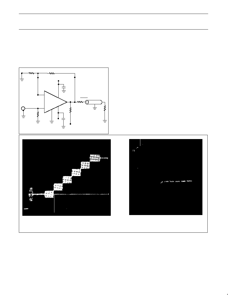
NE5539 COLOR VIDEO AMPLIFIER
The NE5539 wideband operational amplifier is easily adapted for
use as a color video amplifier. A typical circuit is shown in Figure 2
along with vector-scope1 photographs showing the amplifier
differential gain and phase response to a standard five-step
modulated staircase linearity signal (Figures 3, 4 and 5). As can be
seen in Figure 4, the gain varies less than 0.5% from the bottom to
the top of the staircase. The maximum differential phase shown in
Figure 5 is approximately +0.1
∞
.
The amplifier circuit was optimized for a 75
input and output
termionation impedance with a gain of approximately 10 (20dB).
NOTE:
1. The input signal was 200mV and the output 2V. V
CC
was
±
8V.
7
75
750
--V
22nF
14
--
10
8
3
1
+
75
VIN
--V
22nF
470
75
--V
ZO = 75
1
6dB LOSS--1
75
Figure 2. NE5539 Video Amplifier
Figure 3. Input Signal
Figure 4. Differential Gain <0.5%
NOTE:
Instruments used for these measurements were Tektronix 146 NTSC test signal generator, 520A NTSC vectorscope, and 1480 waveform
monitor.

Philips Semiconductors RF Communications Products
Product specification
NE/SE5539
High frequency operational amplifier
April 15, 1992
236
Figure 5. Differential Gain +0.1
o
ZIN = 500
820
220
2≠10pF
+
1
+2V
≠8V
470
8
NE5539
118
87
ZO = 50
14
1K
2K
CLEAD
1.5pF
Figure 6. Non-Inverting Follower
≠
Figure 7. Inverting Follower
+
1
+8V
≠8V
470
8
NE5539
118
87
14
3.3pF
1K
320
2≠20pF
50
1K
≠